
Artificial intelligence is driving unprecedented demand for computing power, placing photonic chips, devices that use light instead of electricity to process data, at the center of the race for next-generation AI hardware. But a stubborn manufacturing bottleneck has kept these chips confined to laboratories: fabricating the complex three-dimensional nanostructures they require has been painfully slow.
Now, a Chinese research team has unveiled a technique that slashes production time from hours to seconds. Published in the peer-reviewed journal Advanced Materials on July 4, the method uses a parallel ion-beam process to fold flat nanostructures into precise 3D shapes across an entire 4-inch wafer in a single, rapid step, achieving a speed improvement of over 100 times compared to conventional techniques.
The Manufacturing Bottleneck That Held Photonics Back
Photonic chips process information using photons rather than electrons, offering dramatically higher bandwidth and lower power consumption than traditional electronic chips. However, their advantage comes at a fabrication cost: photonic devices often require intricate three-dimensional micro- and nano-architectures with nanometric precision.
Until now, the dominant approach for creating these structures has been focused ion beam (FIB) technology. FIB works like a precision milling tool, carving or bending one tiny feature at a time in a serial, point-by-point process. While it offers high resolution, it is painfully slow. Processing and irradiating a region as small as 100 × 100 micrometers, roughly the width of a human hair, requires at least seven minutes. Scaling that to wafer-level production takes hours, making mass manufacturing commercially unviable. Recent advances in quantum photonic chips using single molecules illustrate just how critical scalable fabrication has become, as researchers push photonic technologies toward real-world AI and networking applications.
“A central challenge is the lack of a manufacturing approach that concurrently satisfies the nanometric precision essential for optical functionality and the wafer-scale uniformity and throughput required for scalable production,” the researchers wrote in their paper.
Ion-Beam-Induced Origami: How the New Method Works
The team, led by PhD student Yi Wang under the supervision of corresponding authors Yang Guo and Changzhi Gu at the Institute of Physics, Chinese Academy of Sciences (CAS), in collaboration with the University of Hong Kong and several other Chinese institutions, developed a radically different approach: broad-beam ion beam etching (IBE).
Think of it as origami at the nanoscale. First, the researchers pattern two-dimensional shapes, such as floral motifs, spirals, and butterfly arrays, onto suspended silicon nitride (SiNx) membranes coated with thin gold films using electron-beam lithography. Then, instead of bending each structure one at a time with a focused beam, they expose the entire patterned wafer to a uniform, collimated stream of argon ions.
Here is the key physical mechanism: as the argon ions bombard the surface, they penetrate the material and create a controlled gradient of lattice defects, essentially tiny vacancies and displacements, concentrated near the surface. This localized damage causes differential volumetric expansion, generating a uniform internal stress field that bends the pre-patterned bilayers upward or downward in a single, synchronized step.
The transformation is remarkably fast. Scanning electron microscopy images captured at 10-second intervals during a 20-second IBE cycle show entire arrays of structures folding simultaneously, with floral and butterfly motifs rising from flat 2D patterns into elegant 3D architectures in near-perfect unison.
From Hours to Seconds: Quantifying the Speed Leap
The numbers tell a compelling story. The IBE platform achieves angular uniformity exceeding 97% across the entire wafer and reduces fabrication time by over two orders of magnitude compared to serial FIB methods. To put that in perspective, the EBL patterning step for a 1 × 1 millimeter structure takes no more than 10 minutes, but the actual 2D-to-3D transformation happens within tens of seconds. An equivalent area processed by FIB would require several hours.

IBE vs. FIB: A Comparison of 3D Photonic Fabrication Methods
| Parameter | Broad-Beam IBE (This Work) | Conventional FIB |
|---|---|---|
| Processing mode | Parallel (entire wafer at once) | Serial (point-by-point) |
| Fabrication time (100 μm2) | ~20 seconds | ≥7 minutes |
| Wafer-scale time | Tens of seconds | Hours |
| Angular uniformity | >97% | Low, history-dependent stress |
| Wafer size capability | 4-inch (full wafer) | Limited to micrometers |
| Structural consistency | High; all structures deform uniformly | Irregular, path-dependent deformation |
| Key limitation | Requires EBL pre-patterning | Extremely slow at scale |
Two Devices, One Platform: What the Team Built
To demonstrate the platform’s versatility, the researchers fabricated two functionally distinct photonic devices operating in widely separated spectral bands.
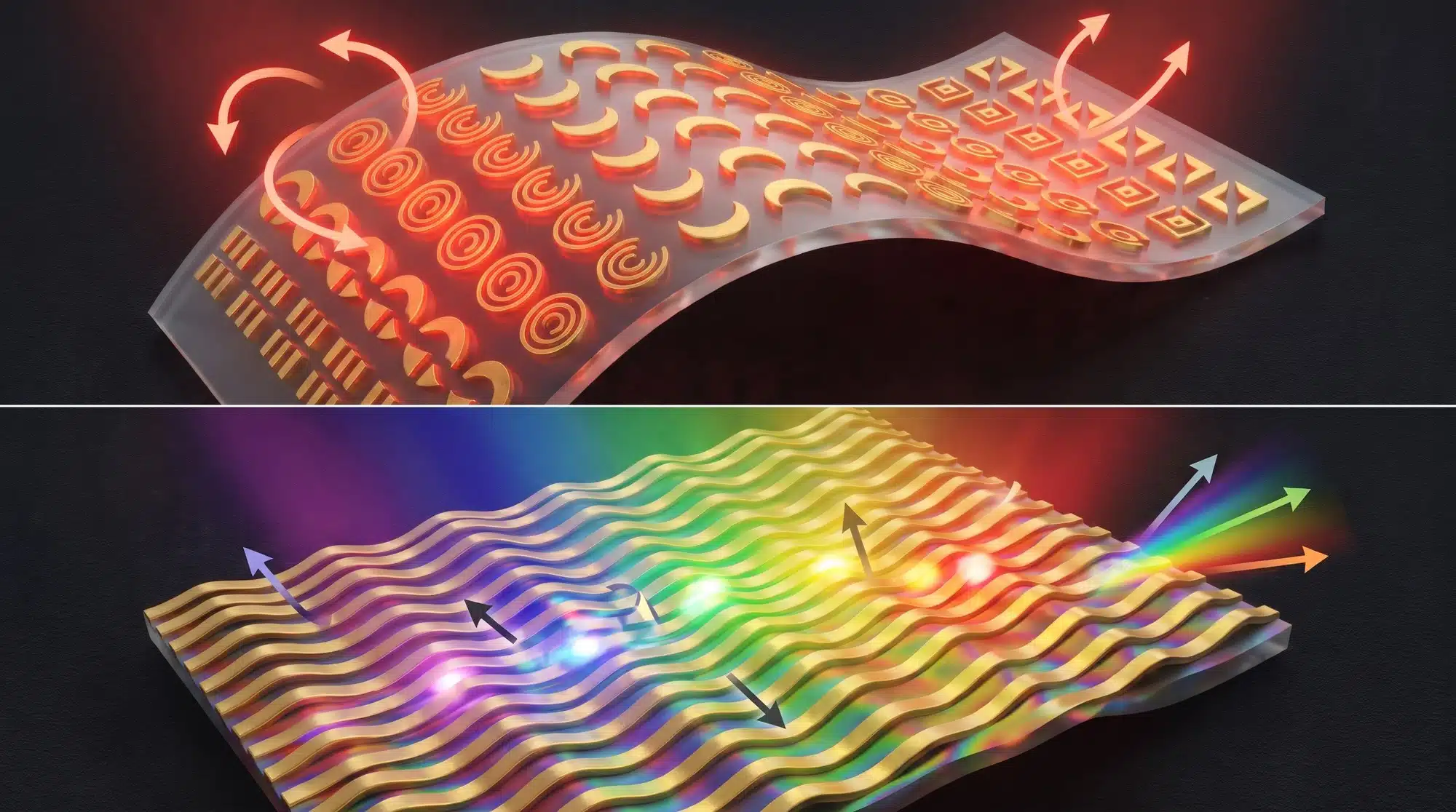
The first is a chiral 3D bending metasurface that achieves a giant experimental circular dichroism (CD) of 0.8 in the mid-infrared at a wavelength of 3.41 micrometers. Circular dichroism, the differential absorption of left- versus right-circularly polarized light, is a valuable property for applications in polarization sensing, chiral molecular detection, and optical communications. A CD value of 0.8 is exceptionally high, indicating that these metasurfaces interact with polarized light in a highly selective and controllable way.
The second device is a collectively buckled plasmonic grating whose resonance is dynamically tunable over 150 nanometers across the visible spectrum via curvature control. This grating supports bound states in the continuum (BICs), a phenomenon where light becomes trapped in the structure even though it exists above the light line, enabling extremely sharp resonances useful for sensors, lasers, and optical filters.
Together, these two devices demonstrate that the IBE platform can produce high-performance photonic components spanning from visible light to the mid-infrared, a remarkable range for a single fabrication technique.
The “Origami” Advantage: Better Performance, Not Just Faster Production
Speed is not the only benefit. The parallel nature of IBE also produces structurally superior devices. When FIB processes curved structures like spirals, the regions exposed first release stress and bend earlier, causing the edges to deform more than the center, a path-dependent inconsistency that worsens with increasing dose. IBE eliminates this problem entirely by delivering ions uniformly and simultaneously, ensuring every structure on the wafer experiences identical conditions.
“Our work establishes a versatile platform that bridges the gap between design complexity and scalable manufacturing for next-generation 3D integrated photonics,” the team wrote.
The technology also substantially expands the application scope of origami architecture, enabling not only individual meta-atoms for 3D metasurface construction but also global buckling modulation of optical response, extending reconfigurable photonic devices from the infrared into the visible regime for the first time.
Why This Matters: Photonic Chips and the AI Revolution
The timing of this breakthrough is no coincidence. AI’s appetite for computation is doubling roughly every few months, and traditional electronic chips are hitting fundamental physical limits. Transmitting data with light rather than electricity offers a path forward: photonic interconnects can carry vastly more data using far less energy, and photonic computing, where light itself performs calculations, promises speed and efficiency gains that silicon cannot match.

Companies like Lightmatter and Intel have been developing photonic chips for AI workloads, while China has been investing aggressively in its photonic ecosystem. As photonic chips move from data-center networking into mainstream computing, manufacturing breakthroughs like this one will become increasingly critical. The IBE technique directly addresses one major barrier to scaling 3D optical chip fabrication: the slow, serial nature of 3D nanostructure fabrication. Another scaling challenge comes from memory, as processors need faster ways to keep working data in the light-based domain. Researchers are now testing foundry-compatible photonic memory as a building block for future optical processors.
China’s Growing Photonic Chip Ecosystem
This breakthrough is part of a broader picture. Over the past year, several Chinese initiatives have advanced photonic chip manufacturing from multiple angles:
- CHIPX TFLN Pilot Line: Launched in June 2025 by Shanghai Jiao Tong University, this production line for thin-film lithium niobate photonic wafers has an annual capacity of 12,000 six-inch wafers, with modulation bandwidth exceeding 110 GHz and ultra-low signal loss.
- Prinano Nanoimprint Lithography: In June 2025, Hangzhou-based startup Prinano validated mass production of photonic chips using vacuum air-cushion nanoimprint lithography, claiming a 90% reduction in manufacturing costs compared to traditional deep ultraviolet lithography.
- SIOM Ultra-High Parallel Optical Computing Chip: Researchers at the Shanghai Institute of Optics and Fine Mechanics (CAS) developed an optical computing chip with over 100 wavelength channels, achieving a theoretical peak computing power of 2,560 TOPS.
- Tsinghua’s Taichi Photonic Processor: Published in Science in 2023, this photonic neural network chip demonstrated AI inference at 3.7 tera-operations per second per watt, orders of magnitude more efficient than electronic GPUs.
The IBE ion-beam origami technique adds a critical piece to this puzzle: a fast, wafer-scale method for creating the 3D structures that many advanced photonic devices require. China has also made parallel strides with wafer-scale 2D chip breakthroughs, signaling a broader push toward next-generation computing architectures.
What Still Stands Between This Breakthrough and Mass Production
While the results are impressive, the technique has limitations. First, the current demonstration uses 4-inch wafers, while commercial semiconductor fabs operate on 8-inch and 12-inch platforms. Scaling IBE to larger wafers will require engineering validation. Second, the patterning step still relies on electron-beam lithography (EBL), which takes up to 10 minutes per square millimeter; it is fast for research but slow for mass production. The researchers note this but point out that EBL is used only for the initial 2D pattern, while the actual 3D transformation is nearly instantaneous.
Integration with existing CMOS-compatible manufacturing processes is another open question. The Au/SiNx bilayer system used in this work is not standard in commercial foundries, and adapting the technique to industry-compatible materials will be an important next step.
Nonetheless, the paper’s key contribution, proving that parallel, wafer-scale 3D nanofabrication of photonic structures is possible, represents a genuine milestone.
Frequently Asked Questions about 3D Photonic Chip Fabrication
What is a photonic chip?
A photonic chip, also known as an optical chip, uses photons (light particles) rather than electrons to transmit and process information. Light travels faster and generates less heat than electrical signals, allowing photonic chips to achieve higher bandwidth and lower power consumption than traditional electronic chips.
Is a photonic chip possible?
Yes. Photonic chips already exist and are used in data centers for optical communications. Companies like Intel, Lightmatter, and Hewlett Packard Enterprise are developing photonic chips for AI computing. The challenge has not been feasibility but manufacturability: making them quickly, cheaply, and at scale.
What is a 3D chip?
A 3D chip uses multiple layers of components stacked vertically, rather than placing everything on a single flat surface. Just as skyscrapers pack more floor space into a small footprint, 3D chips pack more functionality into a compact area. For photonic chips, 3D structures enable complex light pathways, higher component density, and reduced crosstalk between channels.
Is Nvidia working on photonic chips?
Nvidia has invested in photonic interconnect technology through its acquisition of Mellanox and through partnerships with optical component manufacturers, but its core GPU business remains focused on electronic computing. The company is actively researching optical interconnects for data center networking as AI workloads demand ever-increasing bandwidth.
Are photonic chips the future?
Most experts believe photonic chips will complement rather than replace electronic chips. Photonics excels at data transmission and certain computational tasks (particularly matrix multiplication, which underpins AI), while electronics remains superior for general-purpose computing and memory. Hybrid electronic-photonic chips that combine the best of both worlds are widely seen as the most likely path forward.
The Road Ahead
The CAS team’s ion-beam-induced origami technique does not solve every problem in photonic chip manufacturing, but it removes what may have been the most frustrating one: the insane speed gap between what is possible with light and what is practical to build. By proving that 3D photonic nanostructures can be fabricated in seconds across an entire wafer, the researchers have opened a door that many in the industry had assumed would remain closed for years.
As the paper’s authors concluded, their work establishes “a versatile platform that bridges the gap between design complexity and scalable manufacturing for next-generation 3D integrated photonics.” For an industry racing to keep up with AI’s relentless demands, that bridge may prove invaluable.
The study, “Unlocking Wafer-Scale 3D Photonic Systems With Ion-Beam-Induced Origami,” was published in Advanced Materials on July 4, 2026.


