
Semiconductor fabrication represents one of the most demanding manufacturing environments in the world, where the margin for error is measured in nanometers. As chip architectures shrink toward sub-5 nm nodes, the impact of trace-level contamination becomes exponentially more destructive.
Ensuring consistent performance across hundreds of complex processing steps requires a rigorous approach to process control that can identify elemental impurities before they compromise an entire production run. Inductively Coupled Plasma Mass Spectrometry (ICP-MS) has emerged as the definitive analytical solution for this high-stakes environment.
By providing unprecedented sensitivity for trace element detection, ICP-MS semiconductor process control enables fabs to monitor raw materials, ultra-pure water systems, and process chemicals with clinical accuracy. This level of oversight is no longer optional; it is the cornerstone of achieving the high yields and reliability required to power the global digital economy.
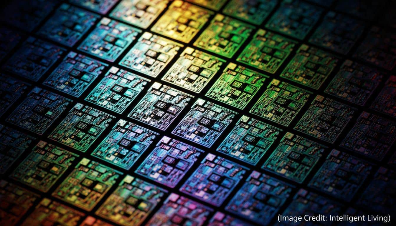
1. Essential Impact of Process Control on Semiconductor Yields
Modern chip fabrication encompasses hundreds of intricate stages, each demanding absolute material purity and a sterile processing environment. Even a slight hint of impurity, such as trace metals in chemicals or particles in gases, can ruin a chip’s performance or destroy its functionality entirely.
Rigorous process control ensures that production materials and procedures remain uniform, predictable, and reliable.
Such vigilance secures optimal yields while minimizing operational overhead, ensuring every component aligns with global quality benchmarks.
2. Strategic Integration of ICP-MS for Elemental Impurity Detection
As a cornerstone of semiconductor process control, ICP-MS provides the sophisticated analytical power required to detect and quantify trace elements at parts-per-billion levels or lower.
Engineers deploy this technology throughout the fabrication facility to oversee processed water integrity, raw material status, and critical production phases. After the integration of ICP-MS, the fabs can:
- Detect impurities in chemicals and gases
- Monitor systems for ultra-pure water
- Test wafers during key phases of production
- Ensure SEMI and ITRS standards with strict rigor are met.
Rapid identification of contamination allows for immediate corrective intervention, preventing localized issues from escalating into widespread wafer loss.
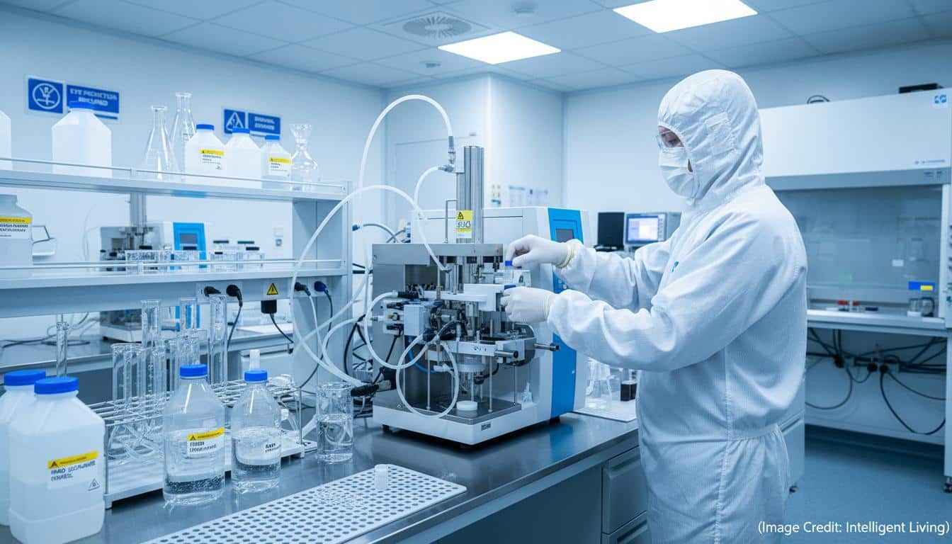
3. Critical Applications of ICP-MS Across the Fabrication Cycle
Here are the key applications of ICP-MS in Semiconductor Process Control:
Raw Material Check
The manufacturing lifecycle begins with high-grade silicon wafers, specialized precursor chemicals, and volatile gases. ICP-MS verifies that every ingredient meets stringent purity thresholds to prevent source-level contamination.
Monitoring of Ultra-High-Purity Water
Fabs rely extensively on ultra-pure water for surface preparation and cleaning; however, even infinitesimal impurities within the UPW stream can degrade the delicate architectures of the wafer. ICP-MS checks that UPW systems can stay free from trace metals and other contaminants.
Control of Process Environment
Etching, deposition, and lithography all require pristine environments to maintain integrity. ICP-MS detects airborne as well as residual contaminants that might have been left from previous operations, ensuring process chambers stay well within safe limits.
Final Product Testing
Before wafers are shipped, ICP-MS is used to check that no harmful trace elements remain. This step acts as a firewall for the reliability of the final product.
4. Measurable Advantages of ICP-MS for FAB Quality Assurance
There are areas where using ICP-MS for semiconductor process control offers significant advantages:
- Unparalleled Sensitivity: Can find the lowest contaminant levels.
- Improved Reliability: Ongoing monitoring ensures stable output.
- Raised Yields: Early detection means less waste and more wafers that can be repaired and sold.
- Regulatory Compliance: Materials meet SEMI, ISO, and international standards.
- Cost Effectiveness: Avoids expensive recalls and delays from substandard products.
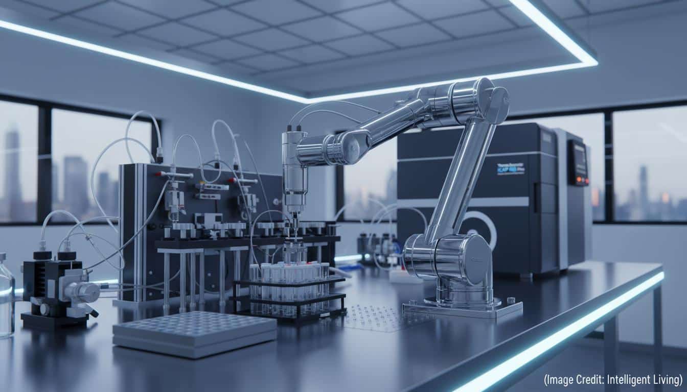
5. Resolving Technical Hurdles in ICP-MS Implementation
Although ICP-MS is an exceptionally powerful tool, it presents unique operational hurdles. While sample preparation remains complex and requires frequent calibration, modern advancements in automated design are significantly streamlining the user experience.
Advancements in Automated Sample Preparation Systems
Transitioning toward full automation or straight-through processing minimizes human error during critical analysis cycles. Real-time monitoring tools further empower fabs to address anomalies immediately, resolving potential issues before they impact large-scale production.
Next-generation analytical platforms now offer configurations tailored specifically for the rigorous demands of semiconductor environments. These specialized systems integrate directly into existing fab-site process control architectures to streamline data acquisition.
6. Evolving Trends in Automated Contamination Monitoring
The industry shift toward smaller nodes and intricate architectures creates an urgent need for advanced contamination control. Next-generation ICP-MS systems will deliver accelerated analysis rates and smarter automation driven by AI-governed data interpretation.
AI-Driven Predictive Modeling for Contamination Avoidance
The surge in data-centric manufacturing protocols ensures that these analytical innovations translate directly into enhanced process stability and repeatable quality. These advancements facilitate immediate reactive measures while enabling predictive strategies that neutralize process anomalies before they manifest.
This predictive foresight redefines production management by ensuring semiconductor manufacturing becomes inherently more robust and efficient.

Advancing Semiconductor Quality Through Analytical Excellence
The integration of ICP-MS semiconductor process control is a transformative shift from reactive troubleshooting to proactive quality assurance. By embedding high-sensitivity trace metal analysis into the fabric of the manufacturing cycle, facilities can safeguard their production lines against the subtle yet devastating effects of elemental contamination.
A steadfast commitment to analytical precision guarantees that every wafer aligns with the rigorous SEMI and ITRS criteria essential for high-performance computing. As we look toward the future of microchip innovation, the role of contamination control will only grow in significance.
The move toward smarter, more automated ICP-MS platforms will provide the real-time data necessary to drive predictive manufacturing models. Ultimately, the ability to maintain absolute purity at every stage of the process will be the deciding factor in which manufacturers lead the next generation of technological breakthroughs.
Frequently Asked Questions on Contamination Control
How does ICP-MS improve semiconductor production yields?
ICP-MS identifies trace impurities in raw materials and chemicals early, preventing defective wafers and reducing costly production waste.
What role does ICP-MS play in ultra-pure water (UPW) monitoring?
It detects parts-per-trillion levels of metallic contaminants in UPW systems to ensure cleaning cycles do not introduce impurities to the wafer surface.
Can ICP-MS detect impurities in semiconductor-grade gases?
Yes, specialized sample introduction systems allow ICP-MS to analyze high-purity gases for metallic contaminants that could disrupt etching or deposition.
Why is trace element detection critical for sub-5 nm chip manufacturing?
At smaller nodes, even a single atom of a metallic impurity can cause electrical leakage or short circuits, making high-sensitivity detection vital.
How do ICP-MS systems support regulatory compliance in fabs?
These systems provide the verifiable data needed to meet international SEMI and ISO standards for material purity and environmental safety.


