
Researchers from Penn State University working in conjunction with Oak Ridge National Laboratory and Lawrence Berkeley National Lab, have developed an atomically thin metal material that will open the door to a wide range of new applications, which include quantum phenomena, biomolecular sensing, catalysis, and nonlinear optics.
Natalie Briggs, a doctoral candidate, and co-lead author said:
We have leveraged our understanding of a special type of graphene, dubbed epitaxial graphene, to stabilize unique forms of atomically thin metals. Interestingly, these atomically thin metals stabilize in structures that are completely different from their bulk versions, and thus have very interesting properties compared to what is expected in bulk metals.
Normally, rust or corrosion occurs when metals are exposed to the air, they incur rapid oxidizing. The paper states that, in as short as one second, metal surfaces can form a layer of rust capable of destroying their metallic properties. When talking about a 2D metal, it would involve the entire layer.
This makes it difficult to combine other 2D materials to metals using a traditional synthesis process because the chemical reactions occurring during the synthesis process ruins both materials. So, the team devised a way to avoid this reaction, by using a single layer of graphene that automatically “caps” the 2D metal during the creation process.
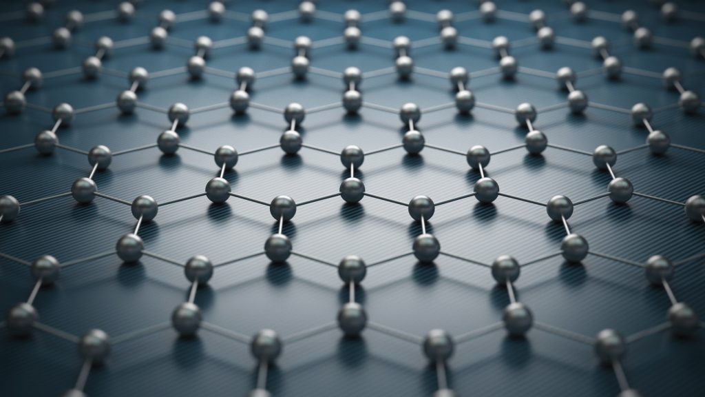
Penn State associate professor of materials science and engineering Joshua Robinson talks about what this means:
In this paper, the focus is on the fundamental properties of the metals that are going to enable a new set of research topics. It shows that we are able to develop novel 2-D materials systems that are applicable in a variety of hot topics such as quantum, where graphene is a key link that allows us to think about combining very different materials that normally could not be combined to form the basis for superconducting or photonic qubits.
They started with silicon carbide heated to a very high temperature, when the silicon leaves the surface the remaining carbon reconstructs into epitaxial graphene. The graphene/silicon carbide interface is only partially stable, which is important because it can be readily passivated by nearly every element if the element has access to this interface.
To provide this access, the team poked holes in the graphene with an oxygen plasma, followed by evaporating pure metal powders onto the surface at high temperatures. This allows the metal atoms to migrate through the holes in the graphene to the graphene/silicon carbide interface, which creates a sandwich structure of graphene, metal, and silicon carbide. The process to create the 2D metals is called confinement heteroepitaxy, or CHet.
Robinson explains why they call it Chet:
We call it CHet because of the confined nature of the metal, and the fact that it is epitaxial — the atoms all line-up — to the silicon carbide, an important aspect to the unique properties we see in these systems.
Next up the researchers look to prove the superconducting, sensing, optical and catalytical properties of the layered materials. Aside from creating 2D metals, they also plan to explore new 2D semiconducting materials with Chet for use in the electronics industry that could be used beyond silicon.


