
Researchers in Taiwan have engineered an interface just 0.42 nanometers thick that could help chips move beyond silicon. The advance, developed by National Yang Ming Chiao Tung University and TSMC Corporate Research and published in Nature Electronics, tackles a long-standing bottleneck in atomically thin transistors. By redesigning the boundary where materials meet, the team achieved strong electrical control without sacrificing electron flow, a balance that has eluded two-dimensional electronics for years. Here is what the breakthrough is, why silicon is reaching its limits, and what it could mean for the future of computing.
What the NYCU and TSMC 0.42-Nanometer Discovery Actually Is
On August 9, 2026, researchers at National Yang Ming Chiao Tung University announced a new transistor design built around monolayer molybdenum disulfide, or MoS2. The semiconductor channel itself is only about 0.7 nanometers thick, essentially one atomic layer.
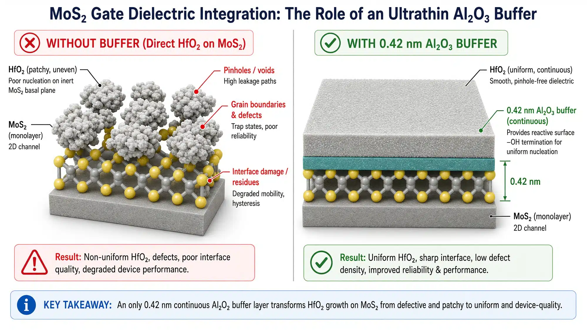
What is new is not the MoS2 itself, but the interface beneath the gate dielectric. The team deposited an epitaxial aluminum layer directly onto CVD-grown monolayer MoS2 in ultra-high vacuum, then oxidized it to form an aluminum oxide layer just 0.42 nanometers thick. On top of that buffer, they deposited a high-k hafnium oxide gate dielectric.
The entire stack achieved an equivalent oxide thickness of about one nanometer with impressive performance: top-gate transistors with channels near 100 nanometers showed low leakage, minimal hysteresis, and a maximum transconductance of 0.45 mS per micrometer.
It is important to be precise. The 0.42-nanometer figure does not describe a 0.42-nanometer transistor or a new manufacturing node. It describes the thickness of the engineered aluminum-oxide interface that makes the rest of the device work better. That distinction matters because the achievement removes a major obstacle to scaling the dielectric system, rather than claiming an entire chip at that dimension.
Why Transistors Have Hit a Wall With Silicon
Silicon has powered Moore’s Law for more than 50 years, but each new generation is now harder to scale. As channels shrink below 5 nanometers, silicon suffers from leakage, weak electrostatic control, and short-channel effects that make it difficult to switch the transistor cleanly.
Industry terminology adds confusion. Names like “5nm” or “3nm” no longer describe the physical gate length. They are marketing labels for generations of process technology. The actual transistor features are larger, and the numbers primarily signal density and performance improvements rather than literal dimensions.
That is why researchers have been searching for channel materials that remain controllable at atomic thickness. Two-dimensional semiconductors are attractive because they can be one to three atoms thick while retaining a defined crystal structure and semiconductor behavior. Their thinness naturally suppresses short-channel effects, which could allow further miniaturization beyond what silicon can sustain at low voltage.

The Atomic Interface Problem That Held Back 2D Transistors
A field-effect transistor needs a gate dielectric, an insulating layer that separates the gate electrode from the channel and controls current flow. Thinning that dielectric improves gate control and helps lower operating voltage, but it also makes the interface more critical.
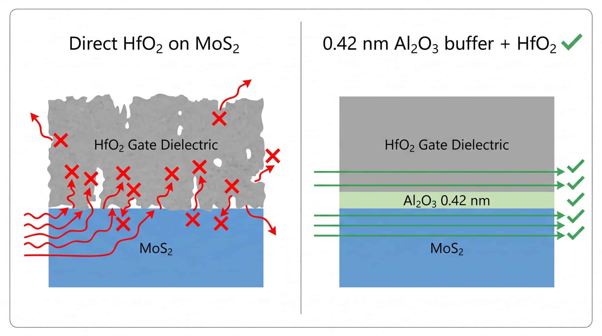
In silicon, decades of refinement have produced high-quality oxidation and deposition processes. Atomically thin semiconductors behave differently. Monolayer MoS2 has a van der Waals surface with no dangling bonds, so deposited dielectrics do not nucleate uniformly. Standard atomic layer deposition can leave gaps, create defects, trap charge, and introduce local electrical disorder.
The result is a classic tradeoff. Engineers could make the dielectric thinner for better control, but the deposition process would scatter carriers and degrade mobility. Or they could protect mobility but sacrifice electrostatic control. Achieving both low equivalent oxide thickness, strong gate coupling, and high mobility at the same time has been especially difficult with wafer-scale CVD-grown MoS2, which is the material most relevant for manufacturing.
Previous workarounds included alternative dielectrics, molecular seed layers, and modified oxide deposition. While each helped, none fully resolved the interface scattering problem at the one-nanometer equivalent thickness regime needed for advanced logic.
How the Engineered 0.42-Nanometer Buffer Works
Rather than inventing a new semiconductor or changing the hafnium oxide itself, the NYCU and TSMC teams re-engineered the three-to-four atom thick boundary between them.
The process has three clear steps:
- Template formation: An ultrathin epitaxial aluminum layer is grown directly on monolayer MoS2 without disrupting the underlying crystal lattice.
- Controlled oxidation: The aluminum is carefully oxidized into amorphous or nanocrystalline aluminum oxide about 0.42 nanometers thick, roughly two atomic layers.
- High-k integration: Hafnium oxide is deposited on the smooth oxide template, forming a uniform gate stack.
The aluminum-oxide layer does two jobs at once. First, it provides a continuous, chemically uniform surface that lets hafnium oxide grow evenly, reducing pinholes and thickness variation. Second, it acts as an atomic buffer that limits unwanted interactions between the high-k dielectric and the MoS2 channel, preserving electron transport.
In the team’s own framing, the interface stops being a passive boundary and becomes an active device element. As Professor Tsung-En Lee noted, when components are only a few atomic layers thick, the interface itself influences how electron states, defects, and bonding environments interact.
Because the demonstration used CVD-grown MoS2 rather than tiny exfoliated flakes, it is also more compatible with large-area processing. Exfoliated flakes are useful in labs but cannot be scaled to wafers. CVD material points toward a path where this interface engineering could eventually be integrated into a manufacturing flow, though uniformity, contact resistance, and reliability across full wafers remain to be proven.
| Approach | Dielectric Quality on MoS2 | Carrier Mobility | Electrostatic Control (EOT ~ 1 nm) | Scalability |
|---|---|---|---|---|
| Direct hafnium oxide on MoS2 | Poor nucleation, gaps and traps | Degraded by scattering | Weak due to leakage and defects | Low |
| Molecular seed layers | Improved but variable | Partially preserved | Moderate | Moderate |
| 0.42 nm epitaxial aluminum oxide buffer + hafnium oxide | Uniform, low leakage, minimal hysteresis | Preserved, high transconductance 0.45 mS per micrometer | Strong at about 1 nm EOT | Higher with CVD MoS2 |
How Small Can a Transistor Get? Understanding Nanometer Limits
The question behind every PAA search about 1nm or 0.5nm chips is simple. What is physically possible?
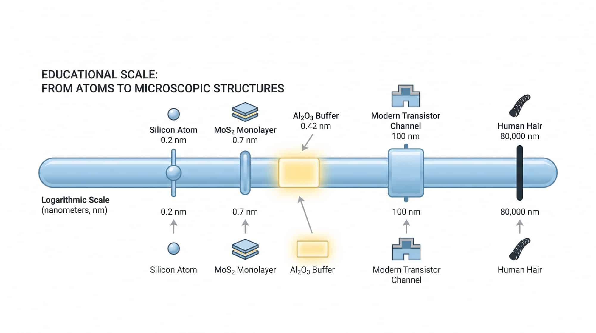
A silicon atom is about 0.2 nanometers in diameter, and a MoS2 monolayer is about 0.7 nanometers thick. A useful transistor cannot be thinner than its atoms and must also include contacts, spacers, and insulators to prevent current from leaking where it should not. Once gate lengths approach a few nanometers, quantum tunneling allows electrons to pass through barriers that should be insulating, raising leakage and power consumption.
That is why the industry separates two concepts:
- Process node name: A label like 3nm or 2nm that describes a technology generation, not a physical dimension.
- Physical thickness or gate length: The actual measured size of a layer or channel, such as the 0.42-nanometer interface or a 100-nanometer channel length.
So, is a 0.5nm or 0.2nm chip possible as a labeled product? No foundry has a 0.5nm node on its roadmap today. TSMC, Intel, and Samsung are ramping 3nm and developing 2nm with gate-all-around architectures. Beyond that, researchers discuss angstrom-scale devices where dimensions are measured in tenths of a nanometer, but these would require new materials, contacts, and lithography far beyond current high-NA EUV.
The more meaningful question is whether transistors can continue to improve without simply shrinking silicon. Two-dimensional channels, interface engineering like the 0.42-nanometer buffer, stacking transistors vertically, and new dielectrics may deliver performance gains even if lateral gate lengths shrink more slowly. For a deeper look at how two-dimensional materials are already being integrated at scale, see our coverage of inside China’s 1-atom thick 2D chips and wafer-scale 2D chip breakthroughs.
Beyond Silicon: What Materials Could Replace It
Silicon will not disappear, but its role as the sole channel material is under pressure. Several families of materials are being evaluated to extend scaling.
- Transition metal dichalcogenides: MoS2, WS2, and WSe2 offer atomically thin channels with good electrostatic control and moderate mobility. They are strong candidates for low-power logic.
- Graphene: Exceptional carrier mobility and thermal conductivity, but it lacks a natural bandgap, which limits its use in digital switching without bandgap engineering.
- Silicon carbide and gallium nitride: Excellent for high-voltage and high-power applications rather than ultra-dense logic.
- Cubic boron arsenide and other emerging crystals: Explored for superior thermal transport to remove heat from densely packed devices.
The reason MoS2 is prominent is not just its thinness. According to the research overview from imec on post-silicon transistors, monolayer transition metal dichalcogenides suppress short-channel effects while remaining compatible with conventional fabrication concepts, and their dangling-bond-free surface, while difficult for dielectrics, also reduces surface roughness scattering.
Choosing a replacement is not a single winner-takes-all decision. Future chips may be heterogeneous, combining silicon for some functions, 2D materials for ultra-scaled logic, and compound semiconductors for power, radio-frequency, and photonic layers.
What This Means for Future Chips, AI, and Energy Use
The immediate impact of the 0.42-nanometer interface is scientific rather than commercial. It proves that electrostatic control and carrier transport can be achieved together at about one nanometer equivalent oxide thickness on CVD MoS2, with 0.45 mS per micrometer transconductance and stable operation. That balance is a prerequisite for low-power logic beyond silicon.
If the approach can be made uniform across wafers, with stable thresholds, low contact resistance, and endurance under thermal and electrical stress, it could feed into several trends:
- Lower operating voltage: Better gate control means transistors can switch with less voltage, cutting dynamic power, which dominates energy use in data centers and AI accelerators.
- Denser, cooler chips: Atomically thin channels generate less leakage in short channels, helping limit heat as transistor density rises.
- Longer Moore scaling: Even without a literal 0.42-nanometer node, interface-level scaling could allow performance gains when lateral shrinking becomes uneconomical.
There are still major hurdles. Contact resistance to 2D materials remains high, wafer-scale defect density must fall, and the aluminum-oxide buffer must survive the full thermal budget of a chip fab. TSMC and NYCU describe the work as an important step, not a manufacturing-ready module, and the interface will need to be co-optimized with gate metals, spacers, and interconnects before it appears in products.
What is clear is the design lesson. As chips approach atomic dimensions, the few atoms where two materials meet matter as much as the materials themselves. Engineering that boundary with atomic precision, as this 0.42-nanometer buffer does, may become a standard tool for extending transistor technology beyond silicon.

Frequently Asked Questions
Is a 0.42 nanometer transistor real?
No, the team did not build a 0.42-nanometer transistor. The 0.42 nanometers refers to the thickness of the engineered aluminum-oxide buffer between the MoS2 channel and the hafnium oxide gate dielectric. The transistors tested had channels near 100 nanometers but with an equivalent oxide thickness of about one nanometer, which is what enables strong gate control.
Is a 1nm transistor possible?
A physical gate length near 1 nanometer faces extreme quantum tunneling and fabrication challenges and is not in production today. The industry’s “1nm” discussions refer to future technology generations that may achieve equivalent performance gains using new architectures like gate-all-around, complementary FETs, and 2D materials, rather than a literal 1-nanometer physical gate.
What is the smallest transistor possible?
In theory, a transistor could be as small as a few atoms, but a practical switchable transistor needs to control current without excessive leakage. Experimental single-atom and molecular transistors exist in labs but lack the reliability, drive current, and manufacturing compatibility needed for commercial chips. For manufacturable logic, most roadmaps aim to extend scaling through materials and structures rather than shrinking silicon gates to sub-nanometer lengths.
Is TSMC 5nm actually 5nm?
No. TSMC’s 5nm and 3nm labels are generation names. They indicate improvements in density, power, and performance over previous nodes, not a measured 5-nanometer gate length. Actual features are larger and vary by design rules. This naming convention is common across all major foundries.
What will replace silicon chips?
There is no single replacement. Silicon will likely remain for many functions, while layered semiconductors like monolayer MoS2, other transition metal dichalcogenides, and potentially new thermal materials are developed for specific layers. The future is likely heterogeneous integration, where different materials are combined to optimize logic, memory, power delivery, and heat removal in the same package.


