
Samsung and AMD signed a memorandum of understanding that goes beyond a typical supplier agreement. The MoU centers on HBM4 memory for AMD accelerators and tuned DDR5 for its next server CPUs and includes language exploring a foundry partnership.
While it appears to be a simple parts deal, the agreement signals a deeper shift toward system-level integration. AI progress is being gated by memory bandwidth, packaging physics, and the ability to scale reliable supply across entire racks; the same kind of physical bottlenecks reflecting data center power and cooling limits dominate scaling decisions.
Partnership between these giants streamlines system-level memory integration for AI clusters. Powering AMD Instinct MI455X accelerators hinges on resolving advanced compute packaging constraints. Exploring a foundry partnership suggests co-designed heterogeneous subsystems to avoid physical limits seen when data center power and cooling limits dominate scaling decisions.

Samsung AMD HBM4 MoU Strategy: Analyzing Terms and Foundry Partnership Exploration
Quick Facts: Samsung-AMD HBM4, AI Memory Supply, and Foundry Exploration
- Deal Scope: AMD ties HBM4 for Instinct MI455X accelerators and optimized DDR5 for 6th Gen EPYC “Venice” to Helios-era rack-scale planning.
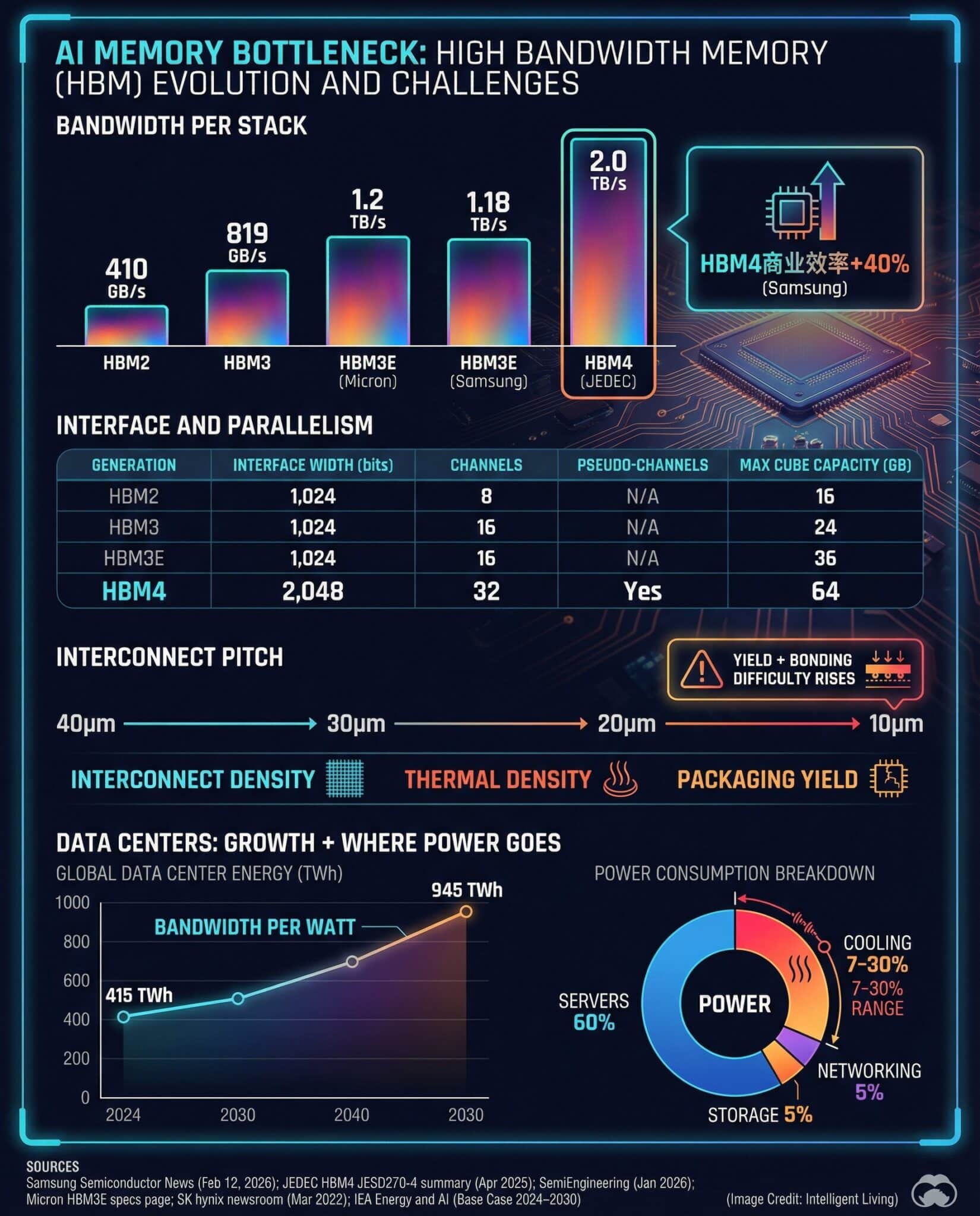
- HBM4 Baseline: A JEDEC-focused view of JESD270-4 HBM4 standard changes highlights wider interfaces and higher per-stack bandwidth ceilings (implementation-dependent).
- Packaging Constraint: The jump from “faster memory” to “usable bandwidth” is constrained by interconnect density and thermals, including how micro-bump HBM and hybrid copper bonding trade off density, yield, and heat removal.
- Rack-Scale Stakes: Rack-scale delivery schedules turn memory qualification into a system requirement, reflected in open rack-scale AI infrastructure collaboration.
Decoding the MoU: HBM4 for AMD Instinct MI455X and EPYC Venice DDR5
In public terms, the MoU confirms Samsung will supply next-generation high-bandwidth memory for AMD’s upcoming Instinct accelerator line. Simultaneously, both companies will tune server memory for the next EPYC platform. A specific clause also covers discussing foundry opportunities that keeps the scope explicitly exploratory. Crucially, “exploring” serves as a planning phrase rather than a manufacturing contract, as it omits specific dies, nodes, or production timelines.
One cloud provider planning manager defines MoUs as “order of operations” documents. Teams align qualification, packaging, and forecasts so the final purchase contract remains predictable and efficient.
What an MoU Is and Is Not
- An MoU signals intent and shared planning assumptions, but it is not the same thing as locked volumes, fixed pricing, or a published production schedule.
- Foundry exploration language signals future intent. Anything beyond “discussing opportunities” stays unconfirmed until both parties finalize specific components and process nodes.
Solving AI Hardware Bottlenecks: Memory Bandwidth and Advanced Packaging Constraints
The HBM4 Memory Standard: Impact on Bandwidth per Watt and AI Performance
What HBM Is, in Plain English
High Bandwidth Memory (HBM) is stacked DRAM placed close to an accelerator die. Proximity allows the processor to pull data significantly faster than conventional DIMM memory. For deeper technical context, AMD’s HBM overview defines why this architecture improves bandwidth per watt versus traditional DDR. Think of it as a fuel line: compute acts as a powerful engine, but a narrow data pipeline forces that engine to idle.
Hardware procurement teams often face “GPU shortages” despite high silicon availability. Stalled bandwidth and memory capacity force expensive compute blocks to remain idle while waiting for data.
What HBM4 Adds
The HBM4 memory standard introduces significant leaps in signaling capability versus HBM3 and HBM3E. Hardware engineers prioritize these specs to ensure accelerators remain fed during peak workloads.
- Interface Width: Moves to a 2048-bit interface, doubling previous standards.
- Bandwidth Ceilings: Enabling bandwidth ceilings around 2 TB/s depending on implementation.
- Commercial Logic: Utilizes a 4nm logic base die to turn specs into volume reality.
Samsung’s roadmap for commercial HBM4 proves how quickly this spec is becoming a market standard.
One practical benchmark is that current accelerator programs already treat HBM bandwidth as a primary design constraint, an idea that shows up in Microsoft’s Maia accelerator baseline.
A common “real life” moment shows up in cluster tuning: an engineer watches utilization graphs and realizes the accelerators are not compute-limited; they are data-movement limited, which is why memory bandwidth becomes the first thing discussed in procurement meetings.

Advanced Compute Packaging: Interconnect Density and Thermal Density Challenges
Why Packaging Matters More than it Used to
HBM4 is not just DRAM stacked vertically. It functions as a heterogeneous subsystem that often includes a logic base die and complex die-to-die interconnect.
Routing, power delivery, test coverage, and heat flow present unavoidable design tradeoffs, making HBM4 memory standard alignment a requirement for system architects. Heterogeneous architecture converts memory into a mixed-node product. Advanced compute packaging has consequently moved from a manufacturing detail to a primary supply constraint. Deployments currently stall when CoWoS-style interposers and advanced substrate capacity bottleneck high-end module production.
Microbumps Versus Hybrid Bonding
Connecting stacked dies requires choosing between two primary technical paths. Each method dictates the final interconnect density and thermal resilience of the package.
- Microbump Solder: Represents a mature, highly scalable industry standard.
- Hybrid Copper Bonding: Aims for higher interconnect density and superior signal behavior.
- Industrialization Pace: Ecosystem readiness decides which method reaches mass production first.
HBM4 roadmaps remain sensitive to these scaling hurdles, explaining why microbump constraints and delayed hybrid bonding adoption dominate current industry packaging discussions.
During a facilities review, one engineer noted that bandwidth promises mean little if the package fails heat or yield targets. Without durability at volume, technical upgrades result in schedule delays.
Why Heat Extraction is the Real Limit
Higher bandwidth drives switching activity and heat generation. As memory stacks become electrically denser, heat extraction grows difficult, frequently driving up system cost and complexity.
Samsung’s packaging stack frames how 2.5D and 3D integration choices impact performance. This includes optimizing performance through heterogeneous integration where thermal management and yield dictate shipping readiness.
Supply risk concentrates alongside packaging capacity. Competitive expansion paths across TSMC, Intel, and Samsung matter as much as raw silicon progress.
Turnkey AI Infrastructure: Foundry Exploration and Helios Rack-Scale Planning
The Foundry Wildcard: What “Exploring Partnership” Could Mean
What Foundry Services Entail
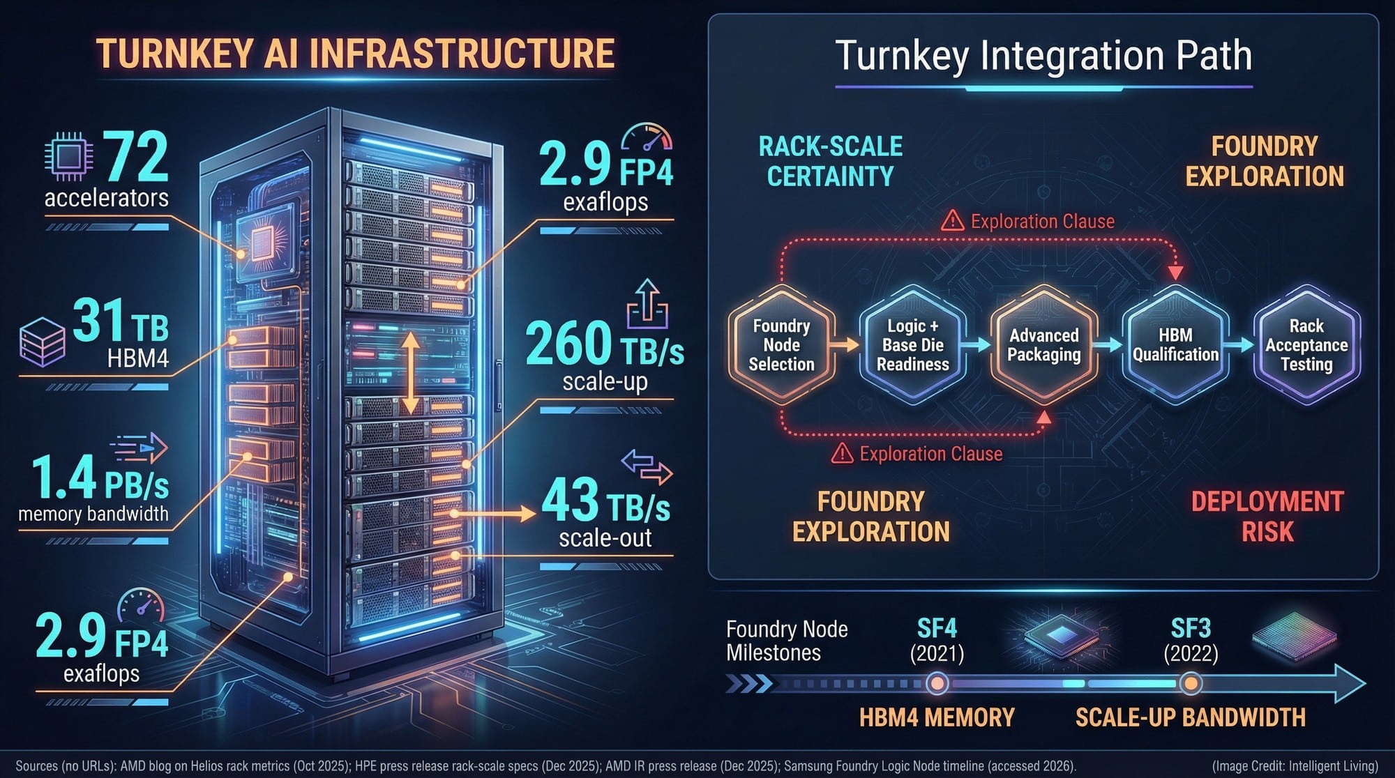
Foundry services cover contract manufacturing of logic dies on specific process nodes, along with associated packaging, test, and qualification services when offered as a combined stack. When those discussions turn concrete, process details matter, including how Samsung defines its SF4 family of logic nodes, which is the level where cost, yield, and performance targets get negotiated. In practice, these projects scale from small chiplets to massive dies, determined by customer qualification needs and foundry reliability.
What We Know and What We Don’t
The MoU language is clear about intent but not scope. It signals that Samsung and AMD want the option to discuss foundry support for next-generation AMD products, but it does not disclose which products, which dies, or which nodes.
Why a Turnkey Stack Appeals to System Builders
The strategic appeal lies in reduced handoff friction. Fewer vendor boundaries between memory, packaging, and manufacturing decisions shorten qualification loops and prevent integration surprises. Samsung markets foundry services alongside integrated package options bundled into a unified manufacturing pipeline. Hardware startup procurement leads view foundry access through several strategic lenses:
- Turnkey Efficiency: One ecosystem for the entire production flow streamlines qualification.
- Vendor Dependency: Concentration within a single stack increases reliance on one provider.
- Long-term Advantage: Early access to co-designed logic and memory provides a competitive edge.
While a turnkey stack reduces handoff friction, it simultaneously creates deeper integration with the chosen manufacturing partner.

Helios Rack-Scale Planning: Achieving Memory Certainty for Next-Gen AI Clusters
Helios and System-Level Guarantees
AMD’s Helios framing treats accelerators, CPUs, and memory as a rack-level system rather than a loose collection of parts. In that model, memory delivery and qualification schedules translate directly into a Helios rack-scale blueprint, where memory planning is treated as a rack-level dependency.
Multi-vendor rack strategies increasingly treat closed stacks and open Ethernet pods as a portfolio decision, which is why dual AI factory planning has become a useful mental model for resiliency.
Two-Tier Memory Architecture
AI systems increasingly rely on a two-tier memory model to balance speed and scale. This split ensures that bandwidth-heavy movement and general orchestration operate on optimized hardware paths.
- Hot Tier (HBM): Dedicated to bandwidth-heavy tensor movement and active compute.
- Host Tier (DDR5): Manages capacity, orchestration, and general-purpose workloads.
- MRDIMM Extensions: Pushes traditional server memory modules toward higher-bandwidth behavior.
These server modules extend the DDR5 ecosystem to meet rising data-movement demands.
When that split shows up in everyday life, it looks like rising RAM pricing and constrained availability, because HBM production competes for wafers and packaging resources that would otherwise feed conventional DRAM, a dynamic captured in global DDR5 supply chain constraints across both enterprise refresh cycles and everyday consumer upgrades.

Future AI Scaling: Memory Pooling, Chiplet Interoperability, and HBM4 Supply Alignment
Scalable AI Clusters: Memory Pooling and CXL Hardware Integration
Why Memory Pooling Is Getting Real Attention
Compute Express Link (CXL) enables pooled memory resources shared across accelerators and hosts. While pooling does not replace HBM’s bandwidth-per-watt role, it reduces overprovisioning and scales capacity efficiently. Consequently, memory pooling in scalable AI clusters is now a core part of rack design conversations.
Rack-level pooling is also becoming a concrete hardware category, including CXL switches for memory pooling, as vendors productize pooled memory fabrics for AI clusters.
Training clusters illustrate this limit. Adding GPUs fails to accelerate training if collective communications bottleneck the system. This is why AllGather and ReduceScatter bottlenecks often stall large-scale GPU performance.
Chiplet Interoperability and UCIe
With packaging now central, the industry is standardizing die-to-die interfaces to ensure chiplets interoperate predictably across different vendors. UCIe provides the specifications for die-to-die interoperability, creating a baseline for easier cross-ecosystem qualification.
Chiplet adoption also improves materials and manufacturing efficiency, improving CoWoS chiplet supply chain efficiency as packaging volumes scale.
Data movement is also colliding with networking limits, which is why photonic chips in data center networking are increasingly framed as a way to move more bandwidth with less heat and loss inside large cluster fabrics.
HBM4 Supply Strategy: Navigating the SK hynix and Samsung AI Rivalry
HBM is a sold-out market in practice, which is why supply certainty increasingly behaves like a product feature. Counterpoint highlights SK hynix leading in revenue share while Samsung fights for market position. In this environment, supply allocation determines which accelerator roadmaps succeed. That is why Samsung’s reported HBM4E qualification for Nvidia’s Rubin Ultra is a development worth tracking.
Scaling AI models often reveals the “memory wall” as a concrete limitation rather than an abstract concept. While compute remains available, data movement often stalls progress. Bandwidth limitations drive interest in monolithic 3D stacking to resolve bandwidth rate-limiting.
Market Indicators: Tracking HBM4 Qualification and Packaging Disclosures
Industry observers must monitor several technical indicators to gauge the success of the HBM4 memory standard transition. Specific markers distinguish marketing roadmaps from verified deployment readiness.
- HBM4 Qualification and Yield: Monitor concrete statements on stack configurations and stable production yields.
- Packaging Disclosures: Watch for bonded approach details, interposer strategies, and thermal design targets.
- Foundry Specifics: Identify when partnership talks name specific dies, nodes, and production timelines.
- Open Pod Momentum: Track how scale-up designs integrate with Ethernet fabrics to see how accelerator pods evolve.
Specific milestones will determine if system builders can achieve the performance targets promised by the Samsung AMD HBM4 MoU.

AI Infrastructure Outlook: Managing Thermal Density and Memory Integration
The Samsung-AMD MoU is a useful signal because it places memory bandwidth, packaging, and supply certainty near the center of AI progress. The practical consequence is that buyers now have to evaluate AI hardware on integration strategy, thermal realism, and delivery confidence, not just peak compute claims.
Rising thermal density shifts cooling from a simple engineering line item to a community resource concern. This is evident in sustainable AI data center cooling, where water access, permitting, and peak load represent significant constraints.
Cooling strategy also shapes siting decisions, especially when operators lean on geography as part of the thermal design, an approach visible in extreme data center locations, where outside air, seawater, and underground layouts become part of the thermal budget.
Efficiency metrics also matter more than slogans. As PUE and WUE become part of the decision stack, energy and water tradeoffs influence where compute gets built and how it is cooled, including data center energy-water constraints, which is why the industry is pushing for higher tokens per watt at every layer.
Grid pressure is part of the same story, because large AI clusters behave like industrial loads, including how AI infrastructure planning affects grid and siting for utilities and permitting. The IEA projects data center electricity demand rising toward 945 TWh by 2030, which makes efficiency and scheduling decisions feel less like IT choices and more like power-system design.
FAQ: Addressing HBM4 Integration and System-Level Hardware Questions
1. How Does Memory Bandwidth Limit AI Accelerator Performance?
Current AI workloads are limited by how fast data moves between the processor and the memory stack. High-bandwidth memory (HBM) solves this by placing DRAM directly next to the accelerator die, reducing latency and boosting bandwidth per watt.
2. What Are the Key Components of the Samsung AMD HBM4 MoU?
The Samsung AMD HBM4 MoU is a strategic framework covering HBM4 supply for AMD Instinct MI455X accelerators, EPYC Venice DDR5 optimization, and foundry partnership exploration. Strategic coordination aims to streamline system-level memory integration for AI clusters.
3. What Technical Gains Does the HBM4 Memory Standard Offer?
HBM4 doubles the interface width to 2048-bit, significantly raising the bandwidth ceiling. High-performance design allows accelerators to maintain higher utilization rates by feeding compute blocks more data without increasing the thermal footprint proportionally.
4. How Does Foundry Exploration Support AMD’s AI Roadmap?
Foundry exploration indicates a potential move toward turnkey manufacturing. Coordinating logic production with Samsung’s 4nm logic base die and advanced packaging reduces integration friction and stabilizes the HBM4 supply alignment.
5. How Does Heterogeneous Integration Manage Thermal Density in AI Hardware?
Utilizing techniques like microbump HBM and hybrid copper bonding allows engineers to create tighter, more efficient connections. These methods improve heat extraction and signal integrity, which are critical as thermal density in AI hardware continues to rise.


